FPGA development |
[HUN] [ENG]
|
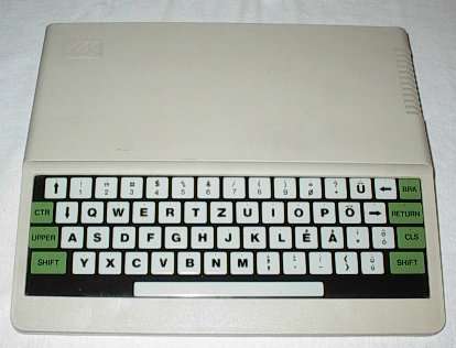
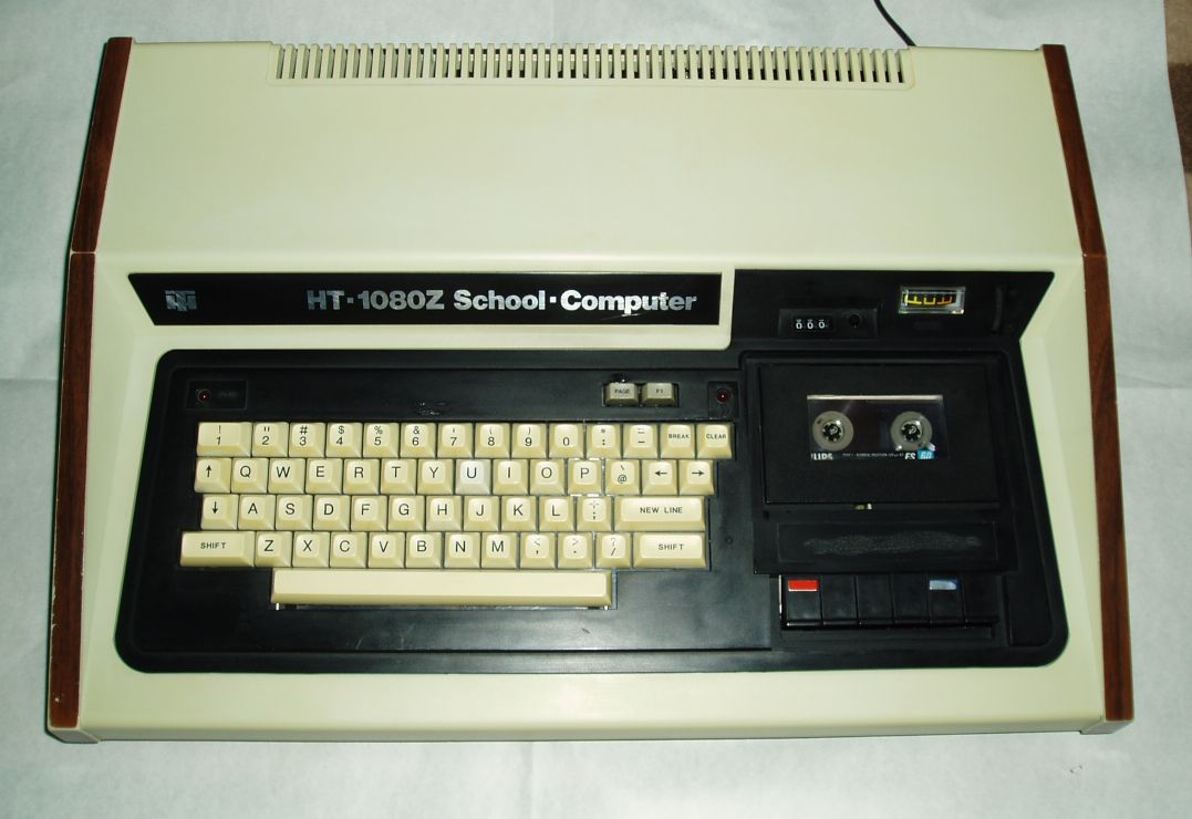
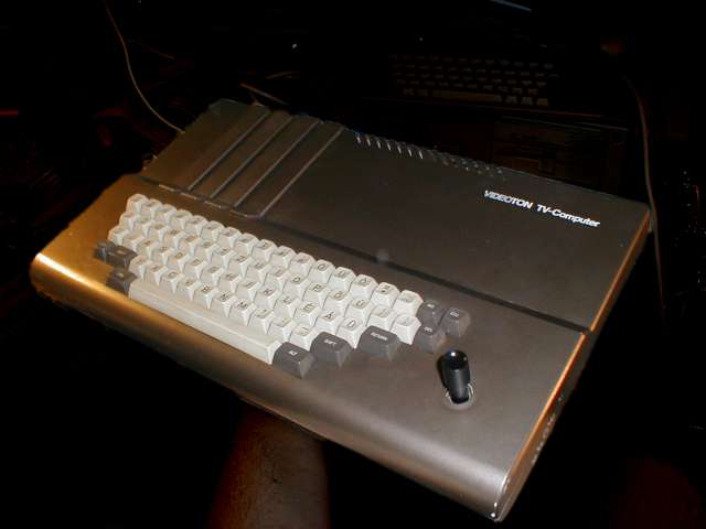
| Primo | HT1080Z | Videoton TVC |
 |
 |
 |
It took years to learn what I know now about the FPGAs. (If you want to know what the FPGAs really are, look around on the Internet). For now, briefly only: FPGAs are highly integrated digital circuits where the internal connection in not fixed, but can vary based on the configuration, which is loaded into the FPGA when it starts. Configuration specifies the internal (actual) connections inside the chip. FPGAs are available in different density and capacity from a couple of thousand gates to millions. At the end, the possibilities are endless, as long as our design fits into a given device.
Besides the classic digital "bricks" (gates, muxes and demuxes, counters, etc.) FPGAs contain special modules as well, which help us to make faster and simpler circuits. Some examples:
- PLL and DCM: Phase-Locked-Loops and Digital Clock Managers help us to generate clock signals, phase shifting and in all the clock related jobs. For example you don't need many external oscillators to have different clocks. One master clock is enough and the PLL/DCM surely can make the other clocks for you. (Well, within certain limits, of course)
- DSP/Muliplier: hardware multipliers and Digital Signal Processors help in high-speed calculations. For example, in your next CPU design you can use one, and the MULT instruction will take only 1T cycle. Neat, is it not?
- Block RAM memory: Internal synchronous static rams are small but very fast. The main purpose of these is creating FIFOs or CACHE modules. Or, you can use as ROM or Video RAM in your work. (As long as the FPGA has enough of them.) True DUAL-PORT feature makes them great indeed. It means that the memory area can be accessed from two individual sides (almost) independently.
- I/O: Different I/O standards are available for the external connections (LVTTL, LVCMOS, PCI, TMDS, DDR). Voltage levels can also vary in a wide range (1.2V, 1.8V, 2.5V. 3.3V). No, there is no 5V tolerant interface though. :-) Special pins can accept different external CLOCKs.
We can choose different ways to design the internal circuits for the FPGA. If someone wants, even schematic drawing is an option, but I don't think it's a good idea. As the complexity grows, soon the designer goes crazy. There must be better ways. This is, where HDL (Hardware Description Language) languages comes into the scope. Designers use two main languages nowadays: Verilog and VHDL. Both have advantages and disadvantages, but the goal is the same: describing how the circuit should work. My opinion is that for beginners, VHDL may be a bit easier. This is what I use, though I can read Verilog, too.
I think it is useful to know the traditional ways of digital designs when we start with FPGAs. Not absolutely necessary, but helps a lot if you know what is a gate and a multiplexer, flip-flop and other "old school stuffs". Perhaps knowledge grows faster if we don't start from "zero", but have some "base" to build on to.
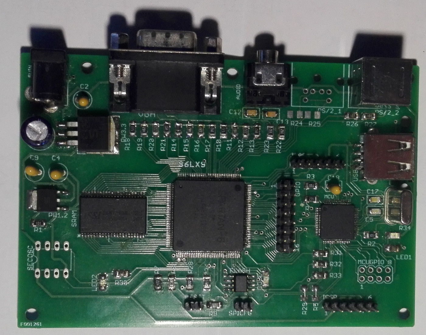
As I worked with FPGAs in the past years, I also leaned to use one circuit designer application, so I could design my own developer board. Well, surely there are cheaper and better commercial boards available on the market, but making your own is such a fun. At the moment I use two boards mainly:
- my own board which has a Xilinx Spartan 6 (LX9)FPGA,
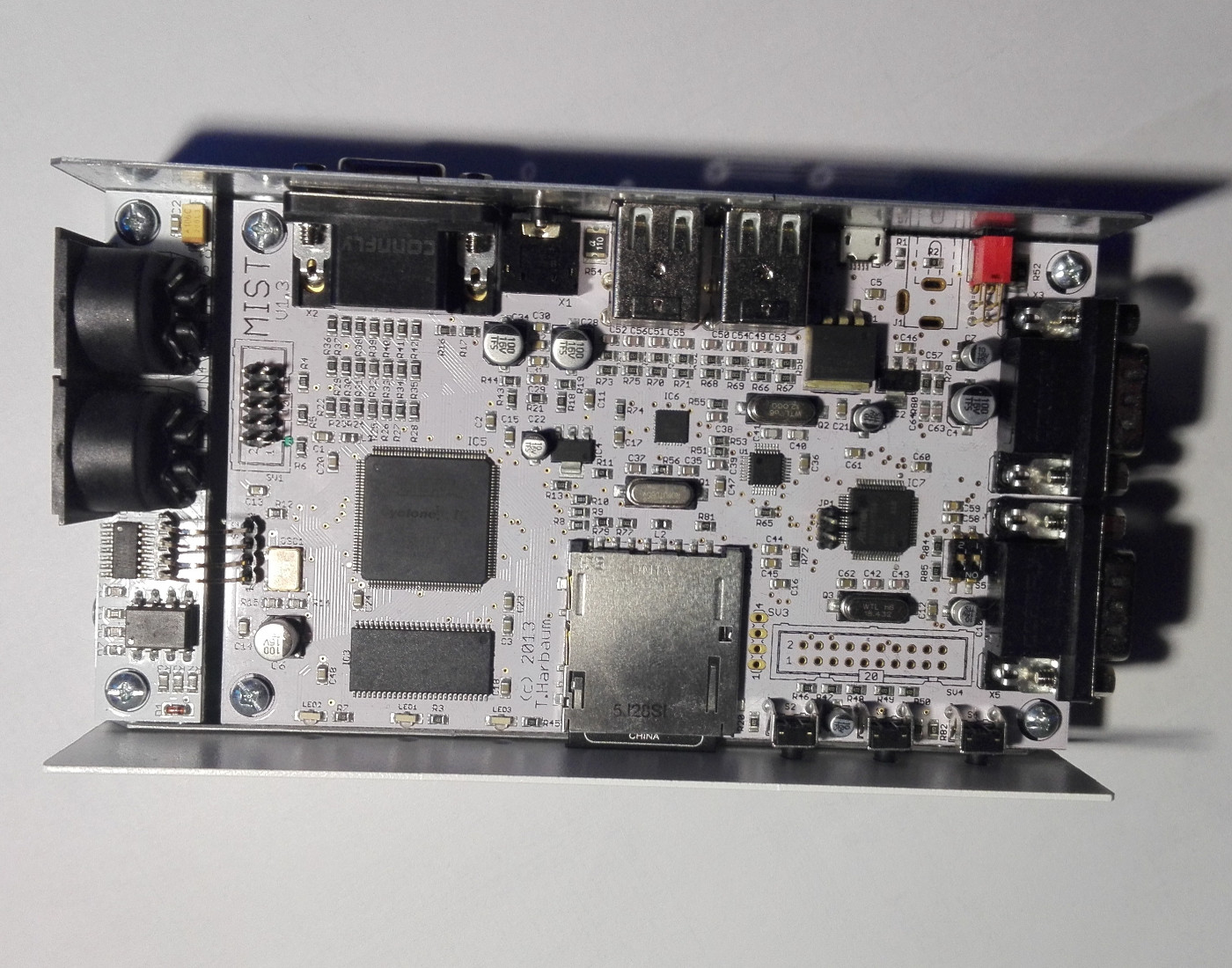
- "the" MiST board with an Altera Cyclone III FPGA.
| The Xilinx Spartan 6 developer board | The MiST board | Implementations: |
 |
 |
Links and references:
[Home]
Contact: write to this email: 